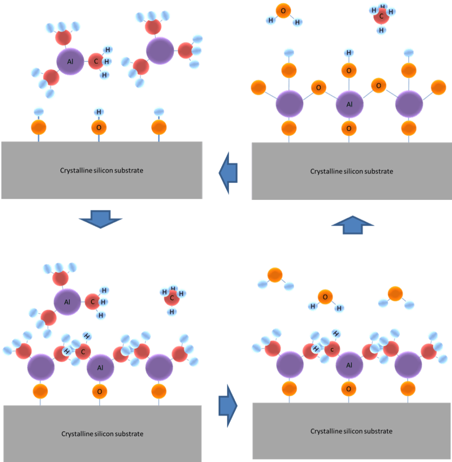
Atomic layer deposition (ALD) is a special case of chemical vapour deposition (CVD) in which the total deposition reaction is split in two or more self-limiting reactions in a sequential way [1]. A special feature of ALD is that the reactant molecules can only react with a limited number of reaction sites at the surface and that the reaction stops once all the reaction sites have reacted. The remaining reactant molecules will not react and will just be pumped from the ALD reactor. Consequently, ALD enables precise and subtle material engineering and the film thickness can be controlled by the number of ALD cycles. Atomic Layer Deposition (ALD) was originally termed atomic layer epitaxy (ALE). The best studied ALD chemistry is the deposition of aluminium oxide using trimethyl aluminium [TMA, Al(CH3)3] and water as shown in Figure 1. In steady-state conditions, the c-Si surface is covered with hydroxyl (OH) groups. The TMA molecule reacts with the hydroxyl groups by splitting off one methyl (CH3) group forming gaseous methane (CH4). Once all hydroxyl groups have reacted, the reaction stops as the TMA molecule cannot react with methyl groups. Subsequently, the remaining TMA molecules, reaction products, and inert carrier gas is pumped from the system. The surface is then exposed to water (H2O) molecules which react with the methyl groups on the surface and form gaseous methane. When all methyl groups have reacted, the surface is covered with hydroxyl groups again and the remaining water, reaction products, and inert carrier gas is pumped from the ALD system. Ideally, one atomic layer is grown per ALD cycle.
There are types of ALD process: thermal ALD and plasma or radical-enhanced ALD. The main benefit of plasma- or radical-assisted ALD is that their significantly higher reactivity which allows for processes to take place at significantly lower temperatures or allows for the growth of materials which are not feasible using only CVD processes. Examples of that are pure metals and some semiconductor materials which need the high reactivity of the radicals (e.g. oxygen or hydrogen) to reduce the parent molecules. ALD processes that can be done using only reactant molecules are referred to as thermal ALD processes.
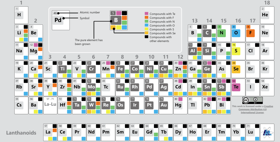
ALD has only recently been introduced in the silicon photovoltaic industry. This was mainly due to the developments in ALD Al2O3 for surface passivation of silicon solar cells [2, 3] as ALD films can yield a better performance for significantly thinner films which is beneficial from a cost point of view. More recently, ALD is also intensively investigated for the deposition of carrier-selective contacts as in this case typically <10 nm films are required with a high conformality. For example, titanium oxide (TiOx) has shown outstanding performance as a surface passivation film [4] and electron selective contact for silicon solar cells [5]. The whole range of materials which can be deposited using ALD is shown in Figure 2, indicating that a very wide range of pure elements, their oxides, nitrides, sulphides, selenides, and fluorides can be grown with all the intrinsic merits of ALD. Hence, ALD could become an even more important technology for silicon solar cell production.
Fundamental thin film growth studies using atomic layer deposition (ALD).
ALD offers unprecedented control of the material composition as the growth precursors that are used during the self-limiting reactions can be easily changed. This allows the synthesis of multilayer structures that can be tailored at the atomic scale towards desired material properties such as work function, phase, density and type of defects, etc. At UNSW we have set up an ALD system with in situ optical emission spectroscopy, quartz crystal microbalance, and spectroscopic ellipsometry. This system uniquely allows the synthesis of a variety of thin films and support the swift integration of these films in various solar cell architectures and materials (e.g. silicon, CZTS and perovskite). This insight can be used to expedite the development of industrial processes, not restricted to ALD.
We are predominantly focusing on synthesising binary metal oxides, such as Al2O3, WO3, MoO3, NiO, SiO2, Nb2O5, TiO2, ZnO and SnO by atomic layer deposition (ALD). We are also developing ternary metal oxide compounds, such as ZnxNi1-xO, AlxNi1-xO, and AlxTi1-xO2 as carrier-selective contacts for silicon solar cells, and ZrxZn1-xO, Zn1-xSnxO, and Mg1-xSnxO (0≤ x ≤ 1) as transparent conducting oxide (TCO) layer for thin film solar cells. We are also keen to work on Al, Si, Ti, Mo, W, Sn, and Ta metals and metal oxide/metal composites once we have hydrogen available in our ALD system.
