Al2O3 provides excellent passivation on p-type c-Si due to its low interface defect density combined with a high negative charge density which offers charge carrier control and is currently the de facto standard for the passivation of the rear of the industrial PERC. Trimethylalu-minium [Al(CH3)3], TMA, is the most commonly used Al-precursor and is often described in idea ALD process. However, the hazards presented by the pyrophoricity of the TMA precursor hindered the introduction of aluminium oxide in the industry and is still a drawback for some companies [1]. An alternative non-pyrophoric Al-precursor, dimethylaluminum isopropoxide (DMAI), has been used to deposit Al2O3 films by metal–organic chemical vapour deposition (MOCVD) [2], PECVD [3] and ALD [4], [5]. Potts et al. have demonstrated the surface passivation of DMAI Al2O3 on both p– and n-type silicon wafers deposited by PE-ALD [5]. However, thermal ALD is preferred for industrial application due to its simple design over much more complex high-volume plasma ALD production.
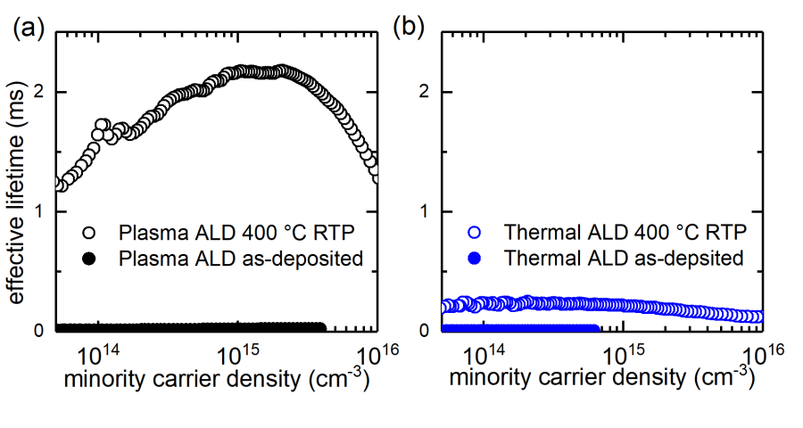
We have studied the surface passivation of DMAI Al2O3 on c-Si deposited by thermal ALD. The passivation of PE- and thermal ALD Al2O3 was evaluated by the injection-dependent effective minority carrier lifetime (τeff) of a symmetrically passivated c-Si wafer. The following graph shows the injection-level dependent effective minority carrier lifetimes of the Al2O3 passivated p-type wafers before and after annealing at 400 ºC. A significant difference between PE and thermal ALD deposited Al2O3 was observed. The origin of the low surface passivation is due to the lack of the SiOx interlayer formation between Al2O3 film and the c-Si substrate identified by Brewster’s angle FTIR technique. This interfacial SiOx is essential to provide chemical passivation.
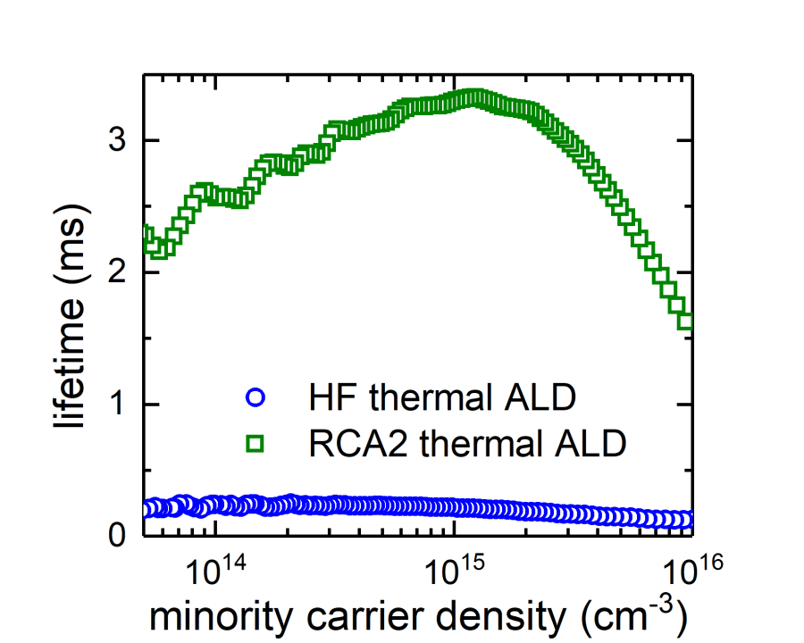
The absence of SiOx is due to the nature of DMAI precursor which is likely to absorb on the c-Si surface without the need of a SiOx layer [6]. Fortunately, this can be solved by applying a chemical grow oxide. In our work, we employed an HCl, H2O2 and water (RCA2) mixture to form a thin (~1.3 nm) SiOx prior to the Al2O3 deposition. This HCl and H2O2 based solution is commonly used in the semiconductor industry to clean the silicon substrate as well as in the PV community. By applying this chemical oxide, the minority carrier lifetime of the p-type FZ wafer could be improved from 0.28 to 3.3 ms, indicating the improvement of the surface passivation, as shown in the following picture. The details of this work can be found in our publication: C.-Y. Lee et al., “Improving the Silicon Surface Passivation by Aluminum Oxide Grown Using a Non-Pyrophoric Aluminum Precursor,” Phys. Status Solidi – Rapid Res. Lett., vol. 12, no. 7, p. 1800156, 2018.
Reference
[2] D. Barreca et al., J. Mater. Chem., vol. 10, no. 9, pp. 2127–2130, 2000.
[3] W. Ban et al., Thin Solid Films, vol. 641, pp. 47–52, 2017.
[6] D.-H. Kim and Y.-C. Kim, J. Nanosci. Nanotechnol., vol. 13, no. 5, pp. 3564–3567, 2013.
